sketch a stick diagram for a cmos 4-input nor gate
Now lets understand how this circuit will behave like a NAND gate. In this video stick diagram of CMOS EX-OR gate is explainedlink for Schematic diagram of CMOS EX-OR gate.
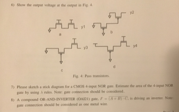
Solved 6 Show The Output Voltage At The Output In Fig 4 D Chegg Com
Estimate the area of your.

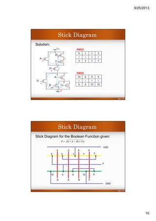
. 1 Answer to Estimate the area of your 4-input NOR gate from Exercise 110. EulerPaths CMOS VLSI Design Slide 4 4-Input NAND Gate Sticks Layout I1 I2 I3 I4 OUT Step 1. What time is aew on tonight uk.
Sketch a stick diagram for a CMOS 4-input NOR gate from Exercise. FOUR INPUT NOR GATE TRUTH TABLE. Sketch a stick diagram for a CMOS 4-input NOR gate 2.
View Homework Help - Exam 1805pdf from MATH 154 at CUNY Hunter College. Order gate wires on poly Step 2. Sci convention dates 2023 warren james jewellers Tech red light violation california cost 2022.
The circuit output should follow the same pattern as. To know what is meant by stick diagram. Solve exercise 110 p58 in the Textbook Question.
000 - VLSI Lecture Series012 - Steps to have Stick Diagram of CMOS. And also Sketch a stick diagram for a CMOS 4-input NOR gate from Exercise 15. Exercise 110 Sketch a stick diagram for a CMOS 4-input NOR gate from Exercise 15.
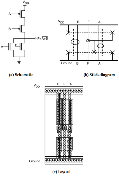
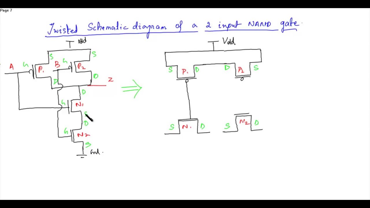
The above drawn circuit is a 2-input CMOS NAND gate. Interconnect Complementary transistor pairs share common. 110 Sketch a stick diagram for a CMOS 4-input NOR gate.
To learn how to draw stick diagrams for a given MOS circuit. Show that the current through. To understand the capabilities and limitations of stick diagram.
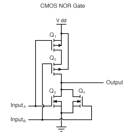
This video demonstrate Layout of CMOS 2 input NAND gate. In this video i have explained Stick Diagram of CMOS NOR Gate with following timecodes. Solve exercise 22 p95 in the Textbook Question.
View the full answer. Electrical Engineering questions and answers.
Ryrpzrf3 Ozglm
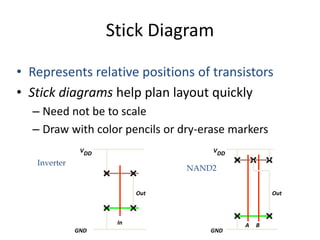
Stick Diagram
How To Draw A Cmos Logic Diagram And Stick Diagram For A B Cd E A Quora

Ppt Introduction To Cmos Vlsi Design Lecture 2 Mips Processor Example Powerpoint Presentation Free To View Id 463b12 Njnmn
Layout Of Logic Gates Digital Cmos Design Electronics Tutorial

Stick Diagram Of Cmos Ex Nor Gate Explore The Way Youtube
Layout Of Logic Gates Digital Cmos Design Electronics Tutorial

31 3 Input Nor Gate Download Scientific Diagram

Stick Diagram Of Cmos Ex Or Gate Explore The Way Youtube
Cmos Gate Circuitry Logic Gates Electronics Textbook

Stick Diagram Of Cmos Nor Gate Cmos Nor Gate Circuit In Vlsi And Digital Electronics Cmoscircuit Youtube
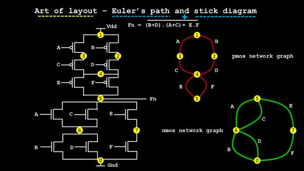
Art Of Layout Euler S Path And Stick Diagram Part 3 Vlsi System Design
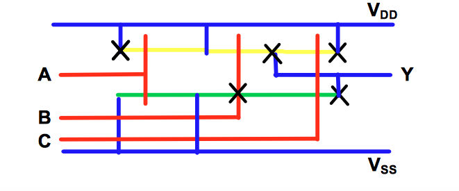
Solved Problem 7 A Stick Diagram Has Been Put Together For A Chegg Com
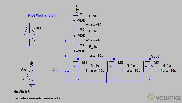
3 Inputs Nor Gate With Cmos Youspice

Cmos Vlsi Design Mips Processor Example Ppt Video Online Download

Norhayati Soin 05 Keee 4425 Week 7 1 23 8 2005 Lecture 9 Keee 4425 Week 7 Cmos Layout And Stick Diagram Cont D Ppt Download
Schematic Diagram And Layout Of Two Input Nand Gate Youtube